 |
|
|
|
|
|
|
|
|
|
|
|
|
|
|
|
Scanning Probe Microscopy (SPM) |
SPM includes a number of techniques for determining physical, electronic, and chemical properties
of nanomaterials and nanodevices. In our lab, we focus on developing new SPM modes that can be
combined with electronic transport measurements to explain the operation of electrical devices.
Kelvin probe force microscopy (KPFM) directly images the surface potentials in a device,
with minimal sample perturbation. KPFM allows us to determine how and where resistance manifests
itself within a nanoscale device. We use this technique to spatially resolve electronic dissipation
due to contact resistances, defect scattering, and electron-phonon interactions.
Scanning gate microscopy (SGM) is a complementary technique that provides additional information
about the localized sensitivity of nanocircuit to electric fields. Using the scanning tip, the
transconductance of a device can be probed to observe inhomogeneities, locally deplete or saturate
the carrier density in specific regions, and isolate the effect of defects or contact barriers.
The Collins group has extended SGM into a spectroscopic tool that we use for identifying specific
electronic states associated with different types of SWNT defects.
|
|
Publications |
Mean free paths in single-walled carbon nanotubes measured by Kelvin probe force microscopy
E.J. Fuller, D. Pan, B.L. Corso, O.T. Gül & P.G. Collins
Phys. Rev. B 89, 245450 (2014).
Quantitative Kelvin Probe Force Microscopy of Current-Carrying Devices
E.J. Fuller, D. Pan, B.L. Corso, O.T. Gul, J.R. Gomez & P.G. Collins,
Appl. Phys. Lett. 102, 083503-5 (2013).
Distinguishing Carbon Nanotube Defect Chemistry Using Scanning Gate Spectroscopy
S.R. Hunt, E.J. Fuller, B.L. Corso & P.G. Collins
Phys. Rev. B 85, 235418 (2012).
Scanning Gate Spectroscopy and Its Application to Carbon Nanotube Defects
S.R. Hunt, D. Wan, V.R. Khalap, B.L. Corso & P.G. Collins,
Nano Lett. 11, 1055-60 (2011).
|
|
Acknowledgements |
| This research is financially supported by the NSF. |
 |
|
|
|
|
|
|
|
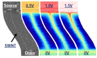
AFM and KPFM images along a SWNT at three different biases.
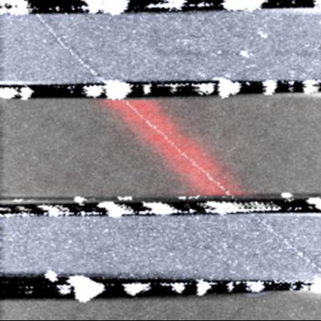 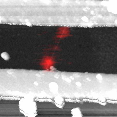
Composite images of topography (grey) and SGM (red), showing that semiconducting SWNTs can have
uniform transconductance due to bandstructure, or concentrated transconductance due to
Schottky barriers.
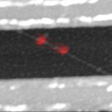
When defects are present, they provide a third, localized type of transconductance.
|
|