 |
|
|
|
|
|
|
|
|
|
|
|
|
|
|
|
Electronic Scattering by Defects |
A focus of our lab is the investigation of defects in one-dimensional SWNTs. A single point
defect introduces resistance, noise, gate sensitivity, and chemical sensitivity to SWNTs. Our lab
combines traditional transport measurements with scanning probe microscopy (SPM) to observe and
understand these electrical consequences.
In transport, it is straightforward to measure the full spectrum of electrical behaviors as a
function of bias and temperature. By measuring the same SWNT before and after incorporation of a
defect, we can often infer the properties of the defect itself.
A more direct technique is to image these sites using our SPM techniques.
In KPFM, we directly image the potential drop that occurs in the vicinity of a defect. These drops
tells us about the extent and strength of scattering around a defect. Due to weak screening in SWNTs,
the scattering barriers and depletion widths surrounding a defect often extend 100's of nanometers, which
can be directly imaged in KPFM.
Using SGM on SWNT defects, we can map the local transconductance) of these sites,
which is also typically proportional to a device's chemical sensitivity.
The SGM technique is extended into a spectroscopy by ramping VG over a wide voltage range, in
order to determine carrier transmission as a function of energy. SWNT defect sites tend to create
a series of transmission maxima and minima dependent on conditions of resonant scattering, and these
peaks can be modified by varying the defect chemistry.
|
|
Publications |
Quantitative Kelvin Probe Force Microscopy of Current-Carrying Devices
E.J. Fuller, D. Pan, B.L. Corso, O.T. Gul, J.R. Gomez & P.G. Collins,
Appl. Phys. Lett. 102, 083503-5 (2013).
Distinguishing Carbon Nanotube Defect Chemistry Using Scanning Gate Spectroscopy
S.R. Hunt, E.J. Fuller, B.L. Corso & P.G. Collins
Phys. Rev. B 85, 235418 (2012).
Scanning Gate Spectroscopy and Its Application to Carbon Nanotube Defects
S.R. Hunt, D. Wan, V.R. Khalap, B.L. Corso & P.G. Collins,
Nano Lett. 11, 1055-60 (2011).
|
|
Acknowledgements |
| This research is financially supported by the NSF. |
 |
|
|
|
|
|
|
|
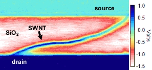
Example KPFM image of a SWNT having a defect.
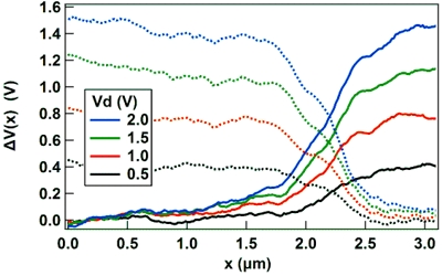
KPFM potential profiles along a SWNT from drain to source, with a large potential drop centered
around a defect site.
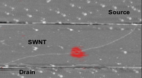
Composite of topography (grey) and SGM (red), showing all of the sensitivity in a
metallic SWNT localized at a defect site.
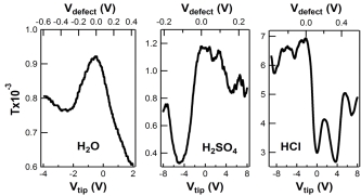
Transmission coefficients through defects created via three different chemistries.
|
|