
Ionic Circuits - Nanofluidic Diode
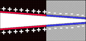
As with any nanopore of small dimension, the surface charge affects the presence of ions inside the pore. In the figure above the right side of the pore would host primarily cations.
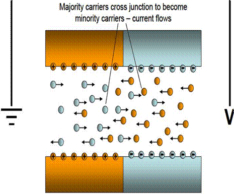
Now what happens at the junction when we apply a voltage?
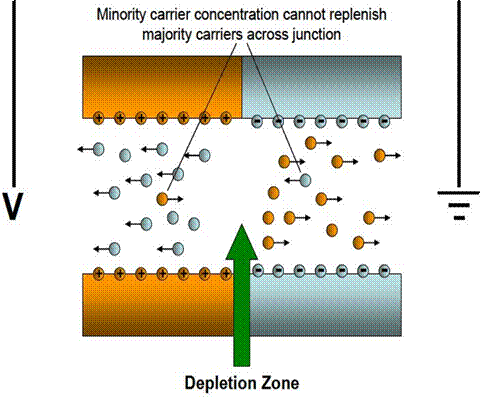
Once a depletion zone has been formed, the current will be drastically reduced. There will still be a small but detectable current due to minority carriers and to a lesser extent hydrolysis of water.
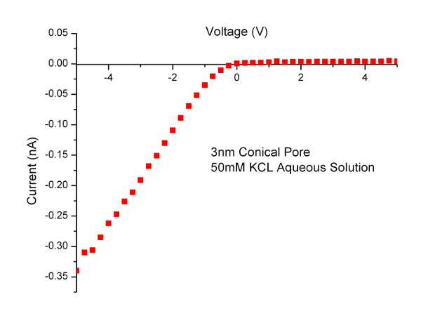
An example IV curve of a modified nanopore acting as a nanofludic diode is shown below. The “forward bias” current values are linear, while the “reverse bias” currents are flat and unchanging with voltage.
Our lab works to make devices analogous to those found in electronic circuits and imporove those we have already made. Other classic electronic devices have also been realized: Nanofludic bipolar transistor and nanofludic field effect transistor are two examples.